The same holds as for my tripod and other diary pages: nothing on this page may be copied or changed and distributed except that the page as a whole may be printed or otherwise transfered in unchanged form, mentioning the original URL and global page reference, and that holds for everyone on the globe and beyond, including so called 'christians' and self-appointed 'Secret Services'.
Home (alt) Tripod Home Local Diary list (Secure) Tripod Diary List Previous Diary
In fact I've asked for new samples after I blew up one sample of the ADS8411 chip I described on my previous local diary page on the same setup, and in fact now I got two of the higher grade ones worth about $30 a piece when one would buy a thousand of them, which I soldered on the adapter board (it's a Conrad one, though I've seen there exist also 'schmartboards' from a califormian company) in place of the old one, which I removed with some effort by a little trick of slicing the pins of with a small sharp hobby knife by pressing down on the top of the pins. The new one just like the old gives me about 8 usefull bits of converted data, depending of course on the source of the input voltage, which is of course not good enough for its normal specs at all, not even close.
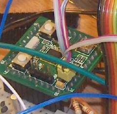
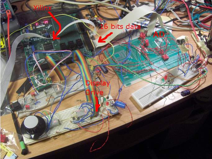
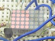
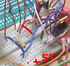
This picture shows the setup:
on the right, the AD converter chip which is the little black centimeter small square connected over the converter PCB lines to the periferial pins, where there are wires to the breadboard below, capacitors (the red blocks) and the flatcable to the Xilinx board input connector.
On the breadboard, there are a supply regulator chip to go from a regulated 5 VOlt supply coming into the board on the right to a 3.3 Digital output pin supply voltage, making the CoolrunnerII chip happy with the AD converter output logic levels, while the AD core is fed with 5 Volts analog circuitry supply voltage.
I think that's where it somehow went wrong with the first chip, because when measuring on the small chip pins with a pointy probe I made a shortciruit in one of the supplies at some point, and after I had connected the board up with the 3.3 Volt supply of the Xilinx board, it somehow has started to pull quite some current, and I found out after a while the little chip package was cooking hot, and after that not really working well anymore. Well, that was a bummer, I didn't even really mess up much, but something must have gone wrong. So I thought I'd ask for new, higher grade samples, which I promply got after 3 or 4 days, from the US, which is nice.
Of course, I though I wouldn't be fooled twice, so I though about strict enforcement of the data from the chips' Absolute Maximum Ratings, also during power up, and preferably also under unforeseen shortcircuit conditions, so I came up with a better supply layout, and some almost good enough setups to let the voltage difference between the 3.3 and 5V supply never become more than the maximum 2.5 volts, in fact by using a heavy transistor and some modern heavy high speed Scotty high frequency diodes and a base emittor diode which simply clamp the voltge difference to less then 2.3 Volts even under shortcircuit currents of 1 amp or higher, and pretty quickly so, and hopefully also when the supply decoupling capacitors of the 5V supply are charging the circuits on the downslope of a shortcircuit. A fast and heavy current diode also prevents all too much reverse voltage buildup when not the 3.3 but the 5V supply is shorted, though not strictly within the absolute maximum ratings, which dictate a max reverse voltage of 0.3Volts, while the diode may easily allow 0.7 V but at least its limited. Of course I'd be able to come up with a circuit which allows less reverse voltage, but that is not trivial enough, and its tricky to make such circuits completely reliable, not current limited (with respect to large decoupling capacitors) and fast enough, to prevent spikes which surge over the limit anyhow.
I've delved into the latest supply regulator chips from TI, and found some NMOS pass transistor based extremely low drop ones, with also very low supply ripple, needing no external capacitors which are good for safe power supply sequencing, for which I've asked samples, too. I might use them at some point, also for audio circuits with low ripple voltage supply.
For those (hihi) which also want to experiment with this technology, don't forget ESD is dangerous for these chips, so you must ground yourself and your workspace in fact, too, to prevent electrostatic discharge from ruining your IO pin circuits subtly.
So does it work now? It seems so, but as I said, it pretty noisy! Now that is nothing special, even an 8 bit AD with a bit of wires connected isn't completely quiet in the sense of +/- 1/2 LSB stable, as I remember from experience from 25 years ago making a AD converter box myself for the school computers. Also the below 12 bits Analog devices microcontroller AD converter is not stable when a unshielded wire is connected to its input of a little length and even when the little stamp board is only measuring its little potmeter voltage it isn't all quiet in 8 or 9 bits, though probably battery feeding it makes it so, if I remember correctly.
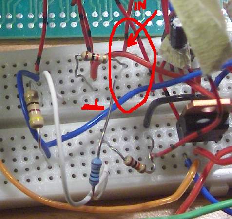
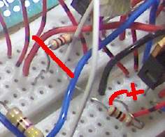
The above image shows the ground connection wire from the adaptor PCB with
the ADS8411 and also it's + input wire, connected to ground with a 1 kilo
ohm resistor (in this case not a metal film one). Under these conditions,
like in the above image, with a clock pulse coming from a low frequency
CMOS schmitt trigger based oscilator, and a simple decoupled internal
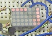
reference voltage for the AD converter, the output can be shown on a 5x7
dot matrix display driven by the Xilinx, which is automatically multiplexed
to display some moving patterns to show the display drive circuitry works,
and to display a 4x4 bit pattern showing 16 input bits of the connector
pins where all 16 output bits of the AD converter are connected to.
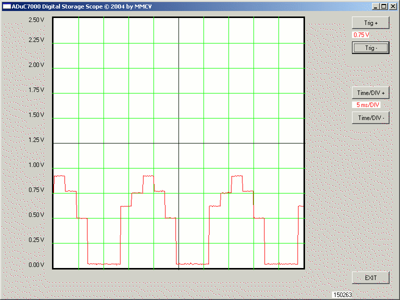
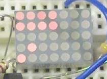
The above image shows the result for the above circuit topology: all lower
left corner 4x4 led dots are on, which means all 16 input bits are 0,
corresponding to the 0 Volt input. The bits are organized as rows of
columns, where the left column contains the highest valued 4 topmost bits,
with the MSb in the upper left corner of the 4x4 block (not taking into
account the highest row of 4 dots, which are fixed to 1 to test the display).
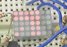
In the following setup, the input has been given a voltage of about 3.3/2 Volts
by a voltage divider of two 1k resistors dividing the 3.3 volt regulated
digital supply:
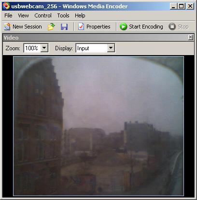
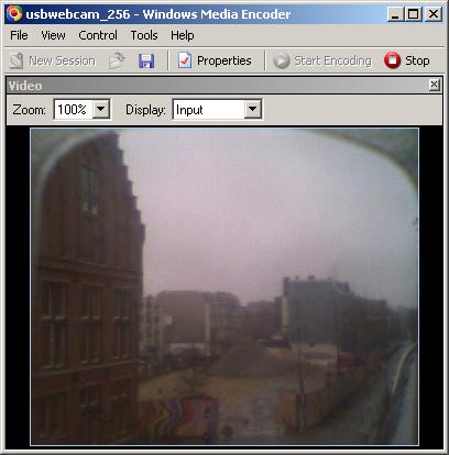
The above image shows one of the resulting binary codes, in this case the highest 8 bits are 01100101, in decimal 101, while we'd want a code according to the input voltage of (3.3/2)*2^16/4.096 or in the case of regarding the 8 nost significant bits: (3.3 Volt input voltage / 2) / 4.096 Volt reference voltage * 256 = 103, which is within the 5% resistor tolerance from the observed value! The lower 8 least significant bits are too noisy, as can be seen from the next picture, taken a little time after the above, from the same circuit with the same input voltage:
The next circuit is the other extreme of the analog to digital converter
input voltage: 5V which is above the maximum input of 4.096 Volts:
Which leads to the anticipated all ones output binary pattern (0xFFFF), the
higherst value:
The noise patterns in the middle example are semi random, though it appears
there are certain prefered patterns when visually inspected, at least there
are no stuck or shortcircuited output bits, they all vary. As I said, the
voltages are only basically decoupled, while in the manufacturers data
sheets, there are seperate, preferably closesy placed decoupling capacitors
for each of the supply pins, also for pins which carry the same voltage,
and then in the evaluation board, there are even 3 (!) values of
parallel capacitors (instead of the common 10 or 100 microFarad parallel
with 0.1uF) per pin! That, and the use of good ground planes, short distance
of the capacitors to the pins and shielding should make more bits relevant
and noise free, like the 13.5 or so which should be relevant according
to the datasheet.
Well, at least it works, and quite properly it seems thus far. It's just very disturbance sensitive, which is natural, 16 bits is a very big dynamic range, check out the relevant bits on your soundcard before jumping to conclusions, those 20 bit converters don't give you a real dynamic range of 2^20 --> 120dB, do they? Or even more hilarious, 24 bits, which should give you 144dB equivalent dynamic range. I haven't seen a single one yet which actually does that. Thats a smallest step of 1 / 16 millionth of the maximum input voltage, pretty darn hard to even analogly buffer, let alone amplify. But they are nice challenges, and this chip then can do its work not with 44.1 or even 192 kilosample per second, but 2MEGA samples per second!
That makes it more sensitive to high frequency disturbance, the input circuit takes a sample in a time of what is it, about 100uSec, and then decouples and starts doing a succesive approximation of the sampled charge on a equivalent of a 25 pF capacitor, so that capacitor must be charged with a 16 bit accurate value... And all variations in supply while the internal digital circuitry starts pounding away to finish only 400nanoSeconds later will influence the SAR value coming out. 13 bits means that a variation of 0.01% will already change a relevant bit. That's a small variation, and high hgh frequencies, little capacitive or inductive couplings start to contribute more and more, like the pulses coming from the 'start convert' clock.
So what to do about all this? Well, an important thing to do in general for these kinds of convertors is to filter the output, which is quite reasonable in the case of an audio converter, which can average a couple of dozen of values, gaining more than a few bits of accuracy, assuming the noise has decent normal distribution. The great advantage of this setup is that the resulting audio signal is sampled so much above the Nyquist rate, that it is most likely very easy to prevent most any aliasing errors at all, 50 times the highest normal audio frequency allows filtering of lets say frequencies higher then a few hundred kiloherz, and then the phase error and the remaining aliasing products can both stay very low.
A major advantage is also the possibility to make a very low latency audio (or other) AD - process - DA loop, because of the very much higher sampling frequency than in normal audio converters. This is because the reconstruction digital and/or analog filter, and the phase problems and pass band behaviour of the anti aliasing filters don't make it necessary to have at least a 1 or a few 44.1kHz samples latency, but only a 50th or so of this very minimum 1 sample (or more) latency. For near field listening (or for instance a headphone feedback) , and most especially for synthesizer applications where a circuit can be put in a loop which feeds back the DA converted output to the AD input, this is an essential property. No one can use ordinary sampled signal processing blocks with analog inputs and outputs in a voltage controlled analog synthesizer setup, and as well as everybody knows that digitally simulated analog synthesizer blocks are not very close to the original, soundwise, because of sampling problems. Also delays of non-submultiples of 44.1 or 48 or 96 or 192 kHz are a lot harder to make with traditional AD/DA converters, and to make a semi-continuous delay based on 2MS/s is a lot easier, even though more memory might be involved: memory is cheap nowadays and often readily available, like the few hundred dollar blackfin DSP boards have 32 or 64 megabytes of reasonably fast dynamic memory. Also, this converter is a simple 'start conversion' triggered device: it doesn't even require an exteral clock signal but only a start convert pulse, which then 400nS later leads to a new sampled output value, so changing the sampling frequency is easy and uncomplicated, and the high sampling frequency should make sure no aliasing or input filtering problems need to take place when sampling with a moderatly varying frequency.
When digital signal paths (like for equalisation) are combined with analog signals grom the same source, a conventional AD/DA setup makes the mix exhibit high frequency phase differences, which makes the frequency response very wrong, and can lead to (comb) phasing effects and distortion increase. The same for effect channels in mixer setups, which are always limited to a fixed minimal delay which is not good for added phasing and chorus effects, which require in that case that the direct signal also be delayed.
The tendency in modern mixers is that the whole signal path becomes digital, which is possible of course, but not exactly cheap or technically pleasing: the AD and DA conversion are seldom really transparent, especially when good high quality HiFi norms are searched for. That tendency of course makes the above considerations not needed, but the effect is that every signal fed into the mixer is delayed a bit which is certainly not always preferable. And in fact, depending on the desired quality, it can be argued that a reconstruction filter which is required for any DA conversion for 44.1 KHz samples might need up to a second or so filtering time for perfect audio quality of the whole audio range. Thats a long delay for a live setup.
Finally, the above circuits should be shielded for 50 Herz mains interference, too, which is obvious: an audio amplifier of that physical layout would also pickup mains hum, as I was reminded of when testing my cookie box shielded audio AD DA converter based on the Burr Brown / Texas Intruments PCM2906 chip, which shows a background noise on a program acting as digital VU meter which is much higher than the perceived noise level because a small 50 Herz hum spoils the measurement. Hence: the metal cookie box. Modern printed circuit boards tend to become smaller and smaller, which helps prevent such electromagnetical interference, and also the use of multiple layers (which one cannot make oneself) on PCBs can make sensitive signals shielded on the PCB.
It is possible to have a practically high dynamic range though, lets take the dynamic range of a microphone, and compare signal strengths with audio power amplifier output levels, than the wires from the microphone can be seen to have lets say a level of about 1 milliVolt, with lets say a modest 60dB lower noise floor (except for spurious transients), while a power amp outputs a voltage of about 25 Volts or so, which is 25000 times higher, so the lowest level differs about 25000000 (25 million) times from the highest in the same system. That's over 146 dB voltage dB difference. But: without a digital pulse factory at micrometers or millimeters or a few centimeters away from the wires picking up those pulses, and those audio disturbances aren't measured as if the spectrum has the range or sensitivity of a GSM antenna.
So what's next? Well, handy enough the AD converter can neatly
be connected up to the Xilinx, which can also be connected to the
blackfin DSp EZLITE board, for which I've programmed decent and fast
interface code already, which appears to work fine, so nothing (except
getting the noise level down) is in the way of doing some signal
processing on a interesting contemporary AD converter signal. Meanwhile
I've also asked TI and received samples of various types of high
quality OpAmps, amoung which what they claim to be the worlds best
audio opamps (very low distortion, low noise, good other audio
properties) and some very fast low noise and some balanced input and
output
operation amplifiers, partwise taken from the Texas Instruments
Evaluation board schematics for a very high quality audio AD converter
(another type: sigma delta converter, stereo 24 bits, over 110dB S/N
and under -100dB distortion (!), up to 200 kS/s DSD super audio signal
option) and from the 8411 evaluation board. A solid, high output
current, accurate, low noise drive opamp should be a good addition to
get some of the disturbance signals down.